Understanding the XC7A100T-2FGG484I and Identifying Common Issues
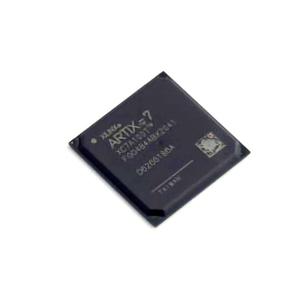
The XC7A100T-2FGG484I is a Power ful and versatile FPGA (Field-Programmable Gate Array) from Xilinx's Artix-7 series. Known for its low power consumption, high performance, and scalability, it is widely used in applications ranging from industrial automation to consumer electronics. However, as with any sophisticated technology, users may face challenges when designing, deploying, or maintaining systems that rely on this FPGA.
1. Power Supply Issues
Power supply problems are among the most common issues encountered when working with the XC7A100T-2FGG484I. These devices require a stable, well-regulated power source to function correctly. Any fluctuations, noise, or insufficient power can lead to unpredictable behavior, including failure to initialize, incorrect output, or overheating.
Solution:
Ensure that the FPGA is powered by a stable voltage source. The XC7A100T-2FGG484I typically requires 1.0V for the core voltage and 2.5V or 3.3V for I/O. Using a high-quality power regulator with appropriate filtering can help maintain stable power. Always measure the power supply with an oscilloscope to ensure clean and stable voltage delivery.
2. Inadequate Clock ing and Timing Issues
Clocking and timing problems are another frequent source of difficulty. The XC7A100T-2FGG484I has multiple clock inputs and internal PLLs (Phase-Locked Loops) that require careful configuration. Improper clock setup can result in timing violations, causing logic errors or system failures.
Solution:
Start by reviewing the FPGA’s clocking scheme. Ensure that all clock constraints are properly defined in the Xilinx Vivado design suite. Double-check the frequency ranges of external clock sources to ensure compatibility. Use Xilinx's timing analyzer tools to check for any violations and address them promptly.
3. Incorrect Pin Assignment
Pin assignment errors are common during FPGA design, particularly when mapping I/O pins for various functions. If the I/O pins are not assigned properly, the FPGA may not communicate correctly with external components, or it may fail to operate altogether.
Solution:
Use the Vivado Design Suite's I/O Planning tools to map the FPGA pins correctly. The XC7A100T-2FGG484I has 484 pins, so proper assignment is critical. Double-check the pin constraints file (.xdc) and verify that it matches the physical connections of your hardware. Always consult the datasheet for the exact I/O characteristics and voltage levels to ensure compatibility with external devices.
4. Insufficient or Incorrect Configuration
The XC7A100T-2FGG484I requires correct configuration to start operating. If the configuration process fails or is incomplete, the FPGA may fail to initialize or may behave unpredictably.
Solution:
Verify that the configuration files (bitstream) are correct and that the programming process is being done through the proper interface (e.g., JTAG, SPI, etc.). Ensure that the FPGA is properly connected to the configuration memory. If you're using a configuration file, ensure it is compiled with the correct bitstream for your specific FPGA configuration.
5. Debugging with Signal Integrity Issues
Signal integrity problems can significantly impact the performance of an FPGA system. Poor signal quality, such as ringing, crosstalk, or reflections, may cause erroneous logic levels or unstable operation, especially at high frequencies.
Solution:
Perform signal integrity analysis using tools like Xilinx’s ChipScope or external oscilloscopes. Pay particular attention to high-speed signal paths such as clock lines and data buses. Use proper PCB layout techniques, including differential pair routing and controlled impedance traces, to minimize signal integrity problems.
Advanced Troubleshooting Techniques for XC7A100T-2FGG484I and Effective Solutions
Once you have addressed basic troubleshooting steps, it's time to dive deeper into advanced techniques that can help resolve more complex issues with the XC7A100T-2FGG484I FPGA. These strategies will ensure your system performs optimally and efficiently.
6. FPGA Logic Errors
Logic errors within the FPGA’s design can arise due to incorrect design implementations, improper initialization of registers, or misinterpreted specifications. These errors might manifest as unexpected output, incorrect timing, or system crashes.
Solution:
Use Vivado's debugging features such as Integrated Logic Analyzer (ILA) or Virtual I/O to monitor internal signals and detect logic errors. Step through your HDL (Hardware Description Language) code to identify any logic issues. Additionally, ensure that the FPGA’s initialization sequence is thoroughly tested and validated.
7. Overheating and Thermal Management
The XC7A100T-2FGG484I is a high-performance FPGA that can generate significant heat under heavy load. Overheating can cause the device to enter a fail-safe state or even permanently damage the chip.
Solution:
Monitor the temperature of the FPGA during operation using a thermal sensor or by checking the thermal performance data from Xilinx. If the FPGA is operating in a thermally stressful environment, consider adding heat sinks, improving airflow, or using active cooling solutions like fans. Thermal management is crucial for high-performance FPGA designs, especially in industrial or automotive applications where reliability is key.
8. Unexpected Reset Behavior
Reset behavior can be difficult to manage in FPGAs. An improper or incomplete reset can leave the system in an unpredictable state, preventing the FPGA from functioning as expected.
Solution:
Ensure that the reset logic is correctly implemented in the design. The reset signal should be stable and applied in a timely manner. Check for any potential conflicts or timing issues in the reset circuit. If using external reset generators or signals, verify their timing relative to the FPGA’s clock to ensure synchronization.
9. High-Speed Interface Problems
Many applications of the XC7A100T-2FGG484I involve high-speed interfaces such as DDR3 memory, PCIe, or HDMI. These interfaces are sensitive to timing, voltage levels, and signal integrity, making them prone to issues if not configured properly.
Solution:
For high-speed interfaces, ensure that the PCB layout adheres to best practices, including controlled impedance traces and proper termination techniques. Use Xilinx's IP cores designed for these interfaces and ensure that the constraints are accurately defined in the design. Use logic analyzers or oscilloscopes to capture signal data and debug communication failures.
10. Inadequate Design Constraints
Sometimes, a failure in the FPGA design isn't due to the FPGA hardware itself but rather improper design constraints. These constraints govern timing, placement, routing, and power consumption, and incorrect or missing constraints can lead to suboptimal performance or errors during implementation.
Solution:
Revisit your design constraints and ensure that all the necessary ones are properly defined. Use Vivado’s Timing Closure tools to check for unmet constraints and optimize your design for performance. Running static timing analysis and reviewing placement and routing can often reveal issues with your current design that are affecting the FPGA’s functionality.
11. Testing and Validation Strategies
Finally, testing and validation are essential steps in troubleshooting FPGA designs. Without thorough testing, it’s difficult to uncover hidden issues that might arise only under specific conditions or load.
Solution:
Develop a comprehensive testing strategy that includes unit testing, integration testing, and stress testing of your FPGA design. Utilize simulation tools to verify the behavior of your design before implementation. For real-time validation, consider using platforms like the Xilinx Vivado Hardware Manager, which can help you monitor the FPGA’s operation and debug in real-time.
By following these troubleshooting steps and solutions, developers and engineers can address the most common challenges faced when working with the XC7A100T-2FGG484I FPGA. Through careful design, configuration, and testing, the chances of encountering significant issues can be minimized, leading to a more efficient and reliable FPGA-based system.
Partnering with an electronic components supplier sets your team up for success, ensuring the design, production, and procurement processes are quality and error-free.


